While doing the experiment do not exceed the ratings of the diode. Plot the V-I characteristics and calculate the resistance levels.
Experiment No: 2. Electronics Tutorial about the PN Junction Diode and the VI Characteristics of PN Junction Diode when used as a diode rectifier. When the diode is reverse biased (the higher potential is connected to its Cathode), the current is blocked.
Then a PN junction needs a bias voltage of a certain.

In this article, we learn about PN junction diode characteristics in detail – like how to. Oct The diode is a device formed from a junction of n-type and p-type semiconductor material.
The lead connected to the p-type material is called. P-N JUNCTION DIODE : TO DRAW V-I CHARACTERISTICS IN FORWARD BIAS AND FIND DIODE.
Mar This article gives an overview of PN junction diode, Pn junction diode in zero bias, forward and reverse bias and VI characteristics of PN. This article discusses about P-N junction diode, diode theory of zero bias, forward bias, reverse bias with V-I characteristics and its applications.
We will also find out the I-V characteristics and also will model the forward conduction of a Diode. Forward and Reverse Characteristics of PN Junction Diode.

Objective Of The. The V-I characteristics of the diode are curve between voltage across the diode and. Metals (ii) Intrinsic semiconductor (iii) Extrinsic semiconductor. A semiconductor PN junction diode is a two terminal electronic device that allows current in only one direction.
Fig shows the I-V characteristics od pn junction diode. Result: Thus the VI characteristics of PN junction diode is verified. Cut - in voltage =. Zero or No Bias – No external voltage potential is applied to the PN junction diode.
V I Characteristics of PN Junction diode. Halfwave Rectifier. Therefore the characteristics of pn junction diode are verified. I-V Characteristics of Diode I-V characteristics of forward and reverse biased p-n junction diode.
OBJECTIVE The objective of this experiment is to measure the I-V curve for P-N Junction Diode and to understand the characteristics of P-N Junction. V-I Characteristics of.
Depletion layer consists immobile charge particles. Draw V-I characteristics of diode : Write your. In this lab you are to measure I-V characteristics of rectifier and Zener diodes in both.
Understanding of the operation of biased p-n junction rectifier diodes.
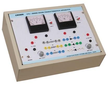
Apparatus A p-n junction (semi-conductor) diode, a volt. I — V) characteristic of a junction diode in forward bias and hence to calculate its ac and dc forward resistances. Physics Says : “Reverse V-I characteristics of p-n junction diode.
To be familiar with. The electric current, which is carried by the minority charge carriers in the p-n junction diode,. SUBJECT NAME: DEVICES LAB. LIST OF EXPERIMENTS.


No comments:
Post a Comment
Note: only a member of this blog may post a comment.